Neurophos Raises $110 Million for Optical Chips: Claims Compute Power at Same Power Consumption is 25x That of GPUs
Author: Sabbir Rangwala
Compiled by: TechFlow
TechFlow Briefing: Austin-based startup Neurophos has developed an Optical Computing Unit (OCU) using silicon photonics and metamaterials, recently securing $110 million in Series A funding led by Gates Frontier with participation from Microsoft’s investment arm M12 and others. The article highlights that its optical core requires no on-chip switches and delivers compute power approximately 25 times greater than a same-sized, same-power-consumption GPU. It projects OCUs will be deployed by 2028 and generate a market around $2.7 billion by 2034—betting on the matrix compute requirements for the AI inference prefill stage and the energy consumption bottlenecks in data centers.
Abstract
Optical computing dates back to 1960 and has matured significantly over the past few decades, performing computations directly in the optical domain. Headquartered in Austin, Texas, Neurophos builds Optical Computing Units (OCUs) using silicon photonic circuits and metasurfaces. The company recently closed a $110 million Series A round to advance its photonic AI chips. Neurophos’s optical core performs instantaneous calculations at the speed of light without internal switches. As a result, it achieves significantly higher operations per second compared to GPUs of identical chip size and power consumption. The potential market is enormous—as OCUs increasingly replace GPUs in data center compute markets. This market is currently estimated at roughly $1 trillion annually.
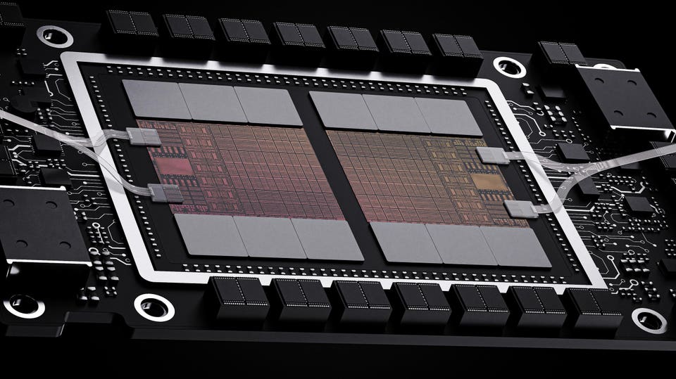
Computing is typically performed on electronic circuits—moving digital bits through transistors, switches, and memory. It is highly efficient and has faithfully followed Moore’s Law regarding scalability, size, power consumption, and speed.
The problem lies in the massive volume of optical data that data centers must process. Traditionally, this data must first be converted to the electrical domain (photons become bits) before being routed through different channels to perform calculations for online searches and the learning and training of AI data streams. The Optical-to-Electrical-to-Optical (OEO) conversion incurs extremely high losses, drastically increasing data center energy consumption and water usage—a costly endeavor financially, politically, and for corporate image. Optical Circuit Switching (OCS) is leveraging silicon photonics and metamaterials to route optical beams, making significant progress in mitigating these expensive OEO conversions. However, computation itself still needs assistance. This is where Neurophos comes in. The company performs computations directly in the optical domain using silicon photonic circuits and metamaterial technology.
Optical computing itself is not new.
It began in 1960: researchers discovered that lenses and optical filters could perform Fourier transforms—a mathematical operation that decomposes a signal or wave into its constituent frequency components.
In the 1970s: Spatial Light Modulators (SLMs) advanced further, enabling programmable generation of optical patterns, focal adjustments, and even directing laser beams along specific paths.
From 1980 to 2000: Two decades saw extensive academic research and innovation, but commercialization remained elusive—primarily due to rapid advances in electronic computing while optics stayed confined to laboratories. SLM technology was later applied to vector-matrix multiplication (VMM), marking a key breakthrough.
From 2000 to 2025: These 25 years witnessed the maturation of optics—optical semiconductors, silicon photonics, metamaterials, fiber optics, and free-space optics, applied to sensing, communications, material processing, and computing. Hyper-scale data centers also rose during this period, consuming vast amounts of optical technology and birthing multi-billion-dollar optical players like Lumentum, Coherent, Corning, and IPG Photonics. Data centers today require optics not just to transmit and switch data, but to "do something" with the data—such as compute. A hyper-scale data center consumes between 100 megawatts and 1 gigawatt of power, with roughly 50% used for computation. Optical computing can drastically reduce this energy draw (and the corresponding cooling demands).
Neurophos is at the forefront of bringing optical computing to reality. Based in Austin, Texas, the company recently raised another $110 million to accelerate optical computing advancements. Led by Gates Frontier, the round included participation from Microsoft’s investment fund M12, Carbon Direct Capital, Aramco Ventures, Bosch Ventures, Tectonic Ventures, Space Capital, among others. This funding enables the company to expand its team by roughly fourfold in 2026. Dr. Patrick Bowen, CEO and Co-founder of Neurophos, stated: "Moore’s Law is slowing, but AI can’t afford to wait. Our breakthroughs in photonics open entirely new dimensions for scaling, packing massive optical parallelism onto a single chip. This physical leap means that efficiency and raw speed scale together, breaking free from the power walls that constrain traditional GPUs. Optical computing redefines what it asks: how much AI we can deliver given a specific power budget, spatial footprint, and cost."
Let’s cover a few fundamentals. Computing during the AI inference phase falls into two categories: "prefill" and "decode." Prefill is the first stage of large language model (LLM) inference, where the model reads and analyzes an entire input prompt in parallel. Decode is when the model generates the response, a highly serial step. In AI inference, prefill dominates the compute load. Training LLMs and running learning processes on massive datasets also generate compute loads; while power-intensive, these represent a brief initial spike during training. The actual training updates consume significantly less power.
Figure 1 contrasts classical optical computing (electrical and GPU-based pathways) and their challenges, alongside how Neurophos solves these problems using its Optical Computing Unit (OCU) architecture.
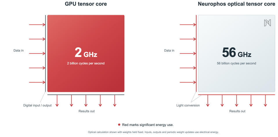
As mentioned, minimizing energy consumption is critical in data center environments. Current computing occurs in the electrical domain, while most data transfer within Scale-Up and Scale-Across racks is already optical. Using electrical GPU chips for computation requires an optical-to-electrical conversion before calculating, followed by an electrical-to-optical conversion for transmission. Transmitting electrons through metal conductors incurs loss. Furthermore, electrical devices like GPUs are packed with switches in their compute cores; waiting for switches to stabilize consumes valuable computation time. In Neurophos’s optical core, calculations complete instantaneously at the speed of light because switches are unnecessary. It executes tens of billions of operations per second across millions of simultaneous calculations, far outpacing a same-sized GPU. Beyond speed, the OCU’s power consumption is significantly lower: no power is needed to drive switches, and signal propagation loss is minimal. Electrical routing and power dissipation are concentrated at the inputs and outputs for electro-optical and opto-electrical conversion. Consequently, at the same chip size and power budget, an OCU completes roughly 25 times more operations per second than a GPU.
Effective photonic storage technologies equivalent to electronics do not yet exist. Therefore, computation must pause, intermediate results must be latched, and the next computation stage begins, advancing mathematical operations discretely, clock cycle by clock cycle. For this reason, SRAM and DRAM are still required. If photonic storage hurdles are overcome in the future, OEO conversion at the OCU’s inputs and outputs would be eliminated, yielding faster speeds alongside reduced power consumption, cost, and footprint.
Prefill calculations involve extensive matrix multiplication, as LLMs establish correlations between prompts and trained weights in high-dimensional spaces. On GPUs, a substantial portion of the chip’s area is dedicated to these operations. On Neurophos’s chip, multiplication is achieved through three operations:
Data copying utilizes optical splitters to divide signals into different paths according to a specific ratio. These are passive components integrable into photonic circuits that split incident photon streams into multiple flows along distinct waveguides, implemented using interferometric couplers, adiabatic tapers, and wavelength-selective gratings.
Multiplication occurs in the optical domain, combining the intensities of multiple light beams using reflective and transmissive structures. Actual optical components include interferometers and phase shifters.
Addition employs optical combiners—components that merge multiple optical signals into a single output stream. They can combine the amplitude, wavelength, phase, or polarization properties of incoming light.
The primary application of optical computing is matrix-matrix multiplication. In optics, one matrix is stored in an optical modulator grid, while the other is fed as a sequence of input vectors, with each numerical value encoded in the amplitude of its corresponding beam. Copying splits each beam into approximately one thousand beams, fanning them out across one row of the modulator grid. Optical multiplication relies on reflection or transmission: each copied beam reflects off the modulators, where the reflected light equals the incident light multiplied by the value stored in that modulator. Addition focuses the light reflected from each column of the grid onto a single photodetector, summing these lights into one output element. Because the modulators maintain their matrix across thousands of input vector passes, the energy to load the matrix is amortized across all those vectors—which is precisely why optical tensor cores are built for matrix-matrix rather than vector-matrix multiplication.
These operations occur on optical chips (as shown in Figure 1), which consist of microscopic waveguides etched into materials like silicon, silicon nitride (SiN), or indium phosphide (InP). Waveguides steer light beams within the chip. Laser sources and photodetectors are integrated into the design to enable OEO conversion. Modulators alter properties of light such as intensity, phase, polarization, and wavelength to encode and process information. Alongside modulators, the waveguides integrate splitters, reflective and transmissive surfaces, and combiners.
Neurophos’s AI inference chips utilize a metasurface architecture featuring tunable optical elements. They target the core constraints of AI infrastructure: manufacturing, powering, cooling, and deploying sufficient compute for hyper-scale inference. Microsoft is deeply involved and serves as an investor. Other commercial partnerships extend to hyper-scale cloud providers. The company has completed computational demonstrations of its first metasurface array and is tape-outing further devices focused on reliability and performance enhancements. The supply chain encompasses leading foundries, custom ASIC designers, optical suppliers, and packaging partners.
A key challenge in optical computing and matrix multiplication is that standard modulators are relatively large, measuring approximately 2 millimeters in length. This means fewer modulators can fit on a chip of a given size, limiting both compute speed and energy efficiency (operations per watt). An array with a thousand modulators on each side only requires two thousand conversions (one thousand in, one thousand out) to execute one million multiplications and one million additions, spreading each conversion across roughly a thousand operations. Neurophos’s "secret" leverages metamaterials to shrink the modulator footprint by approximately ten thousand times compared to state-of-the-art alternatives, allowing one million modulators to fit onto a chip the size of a fingernail rather than a tabletop substrate. This makes thousand-by-thousand arrays feasible on a single chip, finally delivering on the efficiency that optical computing has long promised.
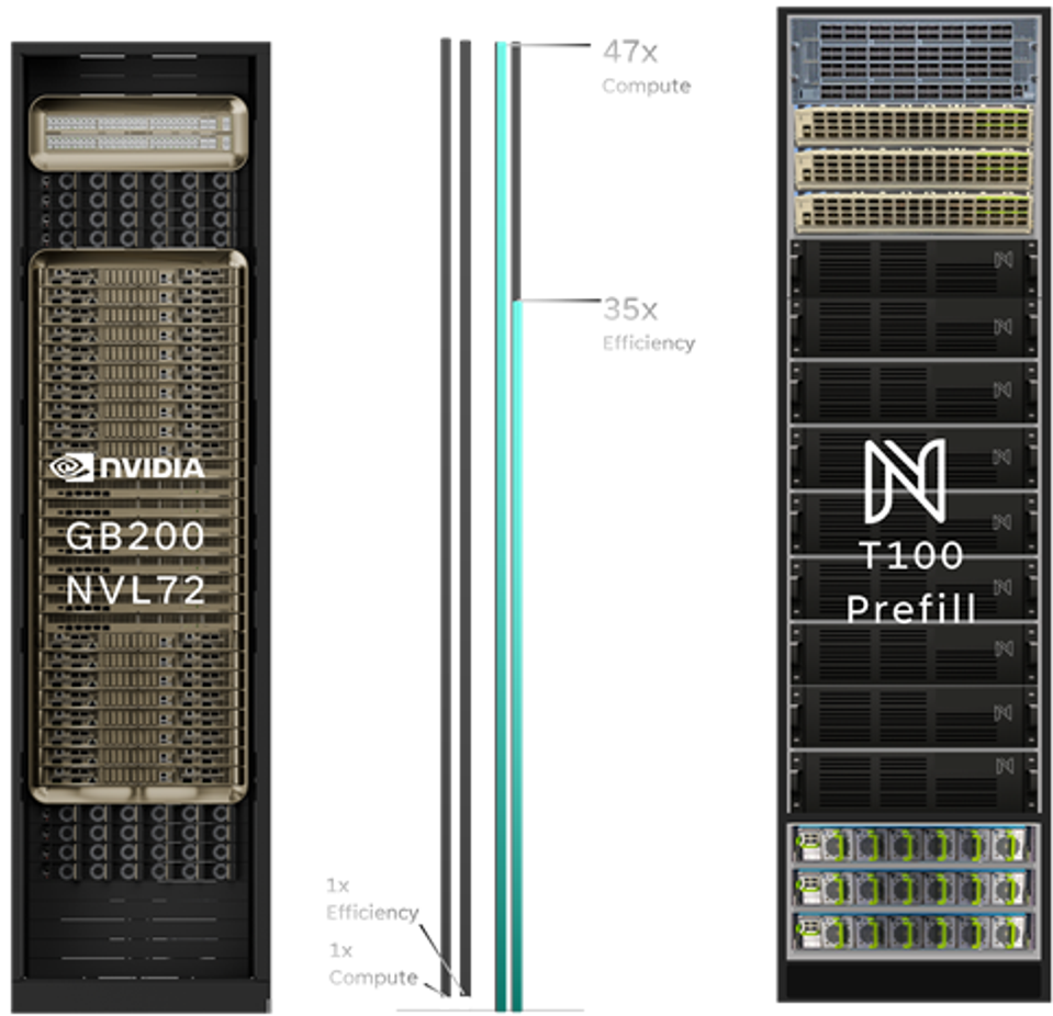
The complete Neurophos optical tensor core comprises a three-part assembly. First, the silicon photonic chip generates input vectors and collects output vectors. It operates on a 56 GHz clock, which dictates compute speed. It utilizes conventional larger modulators but only requires roughly a thousand instead of a million, prioritizing speed over size. Second, the metasurface chip stores the weight matrices. Since the matrix remains constant across numerous input vector passes, these modulators prioritize size reduction over speed. Finally, an optical projection system bridges the two chips: it copies and fans out each input beam from the silicon photonic chip across one row of the metasurface, then focuses the light reflected from each column back onto a single photodetector on the silicon chip to complete the summation. Packaged with High Bandwidth Memory (HBM) and digital chips for control and storage, this optical tensor core becomes a plug-and-play alternative to GPUs. Measured by lithographic mask size die, it runs approximately 50 times faster than today’s most advanced GPUs, with base energy efficiency roughly 35 times higher.
Optics have already become a critical component of data centers; over the next five years, optical integration will continue to rise as Scale-Up racks increasingly adopt Optical Circuit Switching (OCS) rather than Electrical Packet Switching (EPS). The OCS market is projected to grow roughly fivefold over the next five years, reaching $11 billion annually. Another major market lies in computation: relative to electrical pathways like GPUs, OCUs demonstrate significant improvements in compute speed, chip footprint, and power consumption. According to Yole Group, the first wave of OCUs is expected to deploy in 2028, with the market potentially expanding to around $2.7 billion by 2034 (roughly one million units). But the potential extends far beyond that—as OCUs increasingly capture the data center GPU compute market, which is currently estimated at approximately $1 trillion annually.
Join TechFlow official community to stay tuned
Telegram:https://t.me/TechFlowDaily
X (Twitter):https://x.com/TechFlowPost
X (Twitter) EN:https://x.com/BlockFlow_News
 Forbes